
2D Materials for Optoelectronic Devices
Advanced Science
842 views
0 likes
You will need to sign in before you can comment or like.
Nanotechnology involves the synthesis, design, fabrication and application of nanomaterials (size 1-100
nm in any direction). Due to the small size of these particles, they exhibit typical quantum-dynamic phenomenon.
These materials show anomalous electrical, optical and magnetic properties along with quantum-confinement effects.
Nanotechnology has an extremely broad range of potential applications - from nanoscale electronics
and optoelectronics to biological systems and targeted drug delivery.
Conventional drugs used for therapeutic action have limited effectiveness, less sensitivity and
poor distribution. These drawbacks and limitations are overcome by targeted drug delivery,
where polymer nanocomposites, magnetic nanoparticles, carbon nanotubes, plasmonic nanoparticles
are used as nanocarriers.
These nanoparticles serve as a platform to facilitate their specific targeting to cancer cells, minimizing the
risk to normal tissues. Gold nanoparticles can be used to detect early-stage Alzheimer's disease.
Quantum dots are semiconducting nanocrystals that can enhance biological imaging for medical
diagnostics. TiO2, ZnO, SnO2 nanoparticle as mesoporous oxide and CdS, CdSe, ZnS, CuInSe2, CdTe
quantum dot as sensizer find extensively use in solar cell technologies.
Graphene and other transparent conducting metal oxide e.g. CuAlO2 nanoparticles open new doors in the transparent transistor
technologies. Single atom thick graphene film form very high speed transistor. Cadmium selenide
nanocrystals deposited on plastic sheets form flexible electronic circuits. Nanotechnology
based sensors are highly sensitive and selective in detecting very small amounts of chemical vapors,
poisonous gases etc. Carbon nanotubes, zinc oxide nanowires or palladium nanoparticles are used in
such sensors. Because of the small size of nanotubes, nanowires, or nanoparticles,
a few gas molecules are sufficient to change the electrical properties of the sensing elements.
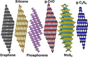
Two dimensional (2D) nanomaterials are considered to be materials where one
of the dimension is less than 100 nm. The story of 2D materials starts with
graphene, which is an allotrope of carbon consisting of a single layer of carbon
atoms arranged in a hexagonal lattice. Graphene is a zero band gap
semiconductor which possess very high electron mobility - as high as 1500 cm2.V-
1.s-1 at room temperature. Being a zero-band gap semiconductor makes it unable to harvest sunlight,
and hence unviable for high performance optoelectronic device applications.
In this context, 2D materials of layered transition metal dichalcogenides e.g.
MoS2, MoSe2, WSe2 are direct band gap (Eg= 1.1-1.9 eV) semiconductors
where the monoatomic layers are stacked vertically with each other by weak Van Der Waals forces.
These types of material are earth abundant which behave like a quantum well
and possess many interesting properties e.g. thickness dependent band
transition, high mobility of charge carriers, high on/off ratio etc. The beauty of
these materials is that they exhibit high charge carrier mobility along with light
harvesting ability. These materials can be used as phototransistors, photodiodes,
photodetectors, spintronic devices etc. These devices form the building blocks for
next generation optoelectronics. Because of their ultrathin nature, they are
easily used for the fabrication of flexible devices which are very compatible for`
use. Also, these materials are cost effective and highly stable for long time at
ambient environment, making them suitable for large scale practical
applications.
Comments